MICRON TECHNOLOGY INC
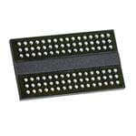
Micron Technology DRAM SDRAMMobile, Part #MT61K512M32KPA-16:C TR | Dynamic random access memory | DEX
Micron Technology DRAM SDRAMMobile, Part #MT61K512M32KPA-16:C TR | Dynamic random access memory | DEX
Shipping calculated at checkout.
Couldn't load pickup availability
Micron Technology DRAM , MT61K512M32KPA-16:C TR
Features
- VDD = VDDQ = 1.35V ±3% and 1.25V ±3%
- VPP = 1.8V –3%/+6%
- Data rate: 14 Gb/s, 16 Gb/s
- 2 separate independent channels (x16)
- x16/x8 and 2-channel/pseudo channel (PC) mode configurations set at reset
- Single ended interfaces per channel for command/ address (CA) and data
- Differential clock input CK_t/CK_c for CA per 2 channels
- Two differential clock inputs WCK_t/WCK_c per channel for data (DQ, DBI_n, EDC)
- Double data rate (DDR) command/address (CK)
- Quad data rate (QDR) and double data rate (DDR) data (WCK), depending on operating frequency
- 16n prefetch architecture with 256 bits per array read or write access
- 16 internal banks
- 4 bank groups for tCCDL = 3tCK and 4tCK
- Programmable READ latency
- Programmable WRITE latency
- Write data mask function via CA bus with single and double byte mask granularity
- Data bus inversion (DBI) and CA bus inversion (CABI)
- Input/output PLL
- CA bus training: CA input monitoring via DQ/ DBI_n/EDC signals
- WCK2CK clock training with phase information via EDC signals
- Data read and write training via read FIFO (depth = 6)
- Read/write data transmission integrity secured by cyclic redundancy check
- Programmable CRC READ latency
- Programmable CRC WRITE latency
- Programmable EDC hold pattern for CDR
- RDQS mode on EDC pins
- Low power modes
- On‐chip temperature sensor with read‐out
- Auto precharge option for each burst access
- Auto refresh mode (32ms, 16k cycles) with per-bank and per-2-bank refresh options
- Temperature sensor controlled self refresh rate
- Digital tRAS lockout
- On‐die termination (ODT) for all high‐speed inputs
- Pseudo open drain (POD135 and POD125) compatible outputs
- ODT and output driver strength auto calibration with external resistor ZQ pin (120Ω)
- Internal VREF with DFE for data inputs, with input receiver characteristics programmable per pin
- Selectable external or internal VREF for CA inputs; programmable VREF offsets for internal VREF
- Vendor ID for device identification
- IEEE 1149.1 compliant boundary scan
- 180-ball BGA package
- Lead-free (RoHS-compliant) and halogen-free packaging
- TC = 0°C to +95°C
MIL:MT61K512M32KPA-16:C TR
MT61K512M32KPA-16:C TR


