TEXAS INSTRUMENTS
Texas InstrumentsPower Switch Ics - power distribution, Part #: TPS22916CLYFPT | Integrated Circuit | DEX
Texas InstrumentsPower Switch Ics - power distribution, Part #: TPS22916CLYFPT | Integrated Circuit | DEX
Couldn't load pickup availability
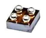
Texas InstrumentsPower Switch Ics - power distribution, Part #: TPS22916CLYFPT features: • Input operating voltage range (VIN): 1 V–5.5 V • Maximum continuous current (IMAX): 2 A • ON-resistance (RON): – 5 VIN = 60 mΩ (typ.), 100 mΩ (85°C max.) – 1.8 VIN = 100 mΩ (typ.), 150 mΩ (85°C max.) – 1 VIN = 200 mΩ (typ.), 325 mΩ (85°C max.) • Ultra-low power consumption: – ON state (IQ): 0.5 µA (typ.), 1 µA (max.) – OFF state (ISD): 10 nA (typ.), 100 nA (max.) – TPS22916BL/CL/CNL (ISD): 100 nA (typ.), 300 nA (max.) • Smart ON pin pulldown (RPD): – ON ≥ VIH (ION): 10 nA (max.) – ON ≤ VIL (RPD): 750 kΩ (typ.) • Slow Timing in C Version Limits Inrush Current: – 5-V turn-on time (tON): 1400 µs at 5 mV/µs – 1.8-V turn-on time (tON): 3000 µs at 1 mV/µs – 1-V turn-on time (tON): 6500 µs at 0.3 mV/µs • Fast timing in b version reduces wait time: – 5-V turn-on time (tON): 115 µs at 57 mV/µs – 1.8-V turn-on time (tON): 250 µs at 12 mV/µs – 1-V turn-on time (tON): 510 µs at 3.3 mV/µs • Always-ON true Reverse Current Blocking (RCB): – Activation current (IRCB): –500 mA (typ.) – Reverse leakage (IIN,RCB): –300 nA (max.) • Quick Output Discharge (QOD): 150 Ω (typ.) (N version has no QOD) • Active low enable option (L versions)
Applications: • Wearables • Smartphones • Tablets • Portable speakers
The TPS22916xx is a small, single channel load switch using a low leakage P-Channel MOSFET for minimum power loss. Advanced gate control design supports operating voltages as low as 1 V with minimal increase in ON-resistance and power loss. Multiple timing options are available to support various system loading conditions. For heavy capacitive loads, the slow turn-on timing in the C version minimizes the inrush current. In cases with light capacitive loads, the fast timing in the B version reduces required wait time. The switch ON state is controlled by a digital input that is capable of interfacing directly with low-voltage control signals. Both Active High and Active Low (L) versions are available. When power is first applied, a smart pulldown is used to keep the ON pin from floating until system sequencing is complete. AFter the ON pin is deliberately driven high (≥VIH), the smart pulldown is disconnected to prevent unnecessary power loss. The TPS22916xx is available in a small, space saving 0.78 mm × 0.78 mm, 0.4-mm pitch, 0.5- mm height 4-pin Wafer-Chip-Scale (WCSP) package (YFP). The device is characterized for operation over a temperature range of –40°C to +85°C.
TEX:TPS22916CLYFPT
TPS22916CLYFPT