XILINX INC.
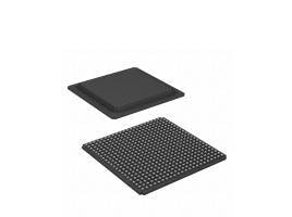
Xilinx Field Programmable Gate Array, Part #: XC3S700AN-4FGG484I | FPGA | DEX
Xilinx Field Programmable Gate Array, Part #: XC3S700AN-4FGG484I | FPGA | DEX
Couldn't load pickup availability
Xilinx Field Programmable Gate Array, Part #: XC3S700AN-4FGG484I combines the best attributes of a leading edge, low cost FPGA with nonvolatile technology across a broad range of densities. The family combines all the features of the Spartan-3A FPGA family plus leading technology in-system Flash memory for configuration and nonvolatile data storage. The Spartan-3AN FPGAs are part of the Extended Spartan-3A family, which also includes the Spartan-3A FPGAs and the higher density Spartan-3A DSP FPGAs. The Spartan-3AN FPGA family is excellent for space-constrained applications such as blade servers, medical devices, automotive infotainment, telematics, GPS, and other small consumer products. Combining FPGA and Flash technology minimizes chip count, PCB traces and overall size while increasing system reliability. The Spartan-3AN FPGA internal configuration interface is completely self-contained, increasing design security. The family maintains full support for external configuration. The Spartan-3AN FPGA is the world’s first nonvolatile FPGA with MultiBoot, supporting two or more configuration files in one device, allowing alternative configurations for field upgrades, test modes, or multiple system configurations.
Features
• The new standard for low cost nonvolatile FPGA solutions • Eliminates traditional nonvolatile FPGA limitations with the advanced 90 nm Spartan-3A device feature set • Memory, multipliers, DCMs, SelectIO, hot swap, power management, etc. • Integrated robust configuration memory • Saves board space • Improves ease-of-use • Simplifies design • Reduces support issues • Plentiful amounts of nonvolatile memory available to the user • Up to 11+ Mb available • MultiBoot support • Embedded processing and code shadowing • Scratchpad memory • Robust 100K Flash memory program/erase cycles • 20 years Flash memory data retention • Security features provide bitstream anti-cloning protection• Buried configuration interface • Unique Device DNA serial number in each device for design Authentication to prevent unauthorized copying • Flash memory sector protection and lockdown • Configuration watchdog timer automatically recovers from configuration errors • Suspend mode reduces system power consumption • Retains all design state and FPGA configuration data • Fast response time, typically less than 100 μs • Full hot-swap compliance • Multi-voltage, multi-standard SelectIO™ interface pins • Up to 502 I/O pins or 227 differential signal pairs • LVCMOS, LVTTL, HSTL, and SSTL single-ended signal standards • 3.3V, 2.5V, 1.8V, 1.5V, and 1.2V signaling • Up to 24 mA output drive • 3.3V ±10% compatibility and hot swap compliance • 622+ Mb/s data transfer rate per I/O • DDR/DDR2 SDRAM support up to 400 Mb/s • LVDS, RSDS, mini-LVDS, PPDS, and HSTL/SSTL differential I/O • Abundant, flexible logic resources • Densities up to 25,344 logic cells • Optional shift register or distributed RAM support • Enhanced 18 x 18 multipliers with optional pipeline • Hierarchical SelectRAM™ memory architecture • Up to 576 Kbits of dedicated block RAM • Up to 176 Kbits of efficient distributed RAM • Up to eight Digital Clock Managers (DCMs) • Eight global clocks and eight additional clocks per each half of device, plus abundant low-skew routing
XLX:XC3S700AN-4FGG484I
XC3S700AN-4FGG484I


