XILINX INC.
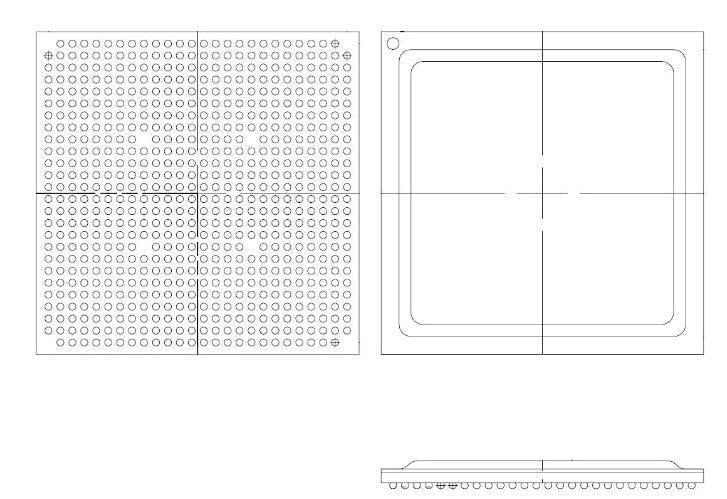
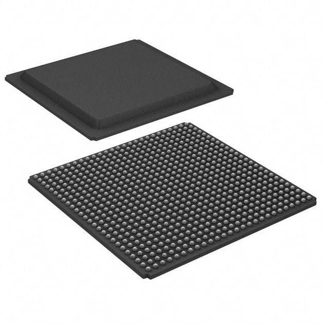
Xilinx Field Programmable Gate Array, Part #: XC4VLX40-10FF668I | FPGA | DEX
Xilinx Field Programmable Gate Array, Part #: XC4VLX40-10FF668I | FPGA | DEX
Couldn't load pickup availability
The Xilinx FPGA #XC4VLX40-10FF668I combines Advanced Silicon Modular Block (ASMBL™) architecture with a wide variety of flexible features, the Virtex®-4
family from Xilinx greatly enhances programmable logic design capabilities, making it a powerful alternative to ASIC
technology. Virtex-4 FPGAs comprise three platform families—LX, FX, and SX—offering multiple feature choices and
combinations to address all complex applications. The wide array of Virtex-4 FPGA hard-IP core blocks includes the
PowerPC® processors (with a new APU interface), tri-mode Ethernet MACs, 622 Mb/s to 6.5 Gb/s serial transceivers,
dedicated DSP slices, high-speed clock management circuitry, and source-synchronous interface blocks. The basic Virtex-4
FPGA building blocks are enhancements of those found in the popular Virtex, Virtex-E, Virtex-II, Virtex-II Pro, and
Virtex-II Pro X product families, so previous-generation designs are upward compatible. Virtex-4 devices are produced on a
state-of-the-art 90 nm copper process using 300 mm (12-inch) wafer technology.
Features
• Three Families — LX/SX/FX
- Virtex-4 LX: High-performance logic applications solution
- Virtex-4 SX: High-performance solution for digital signal
processing (DSP) applications
- Virtex-4 FX: High-performance, full-featured solution for
embedded platform applications
• Xesium™ Clock Technology
- Digital clock manager (DCM) blocks
- Additional phase-matched clock dividers (PMCD)
- Differential global clocks
• XtremeDSP™ Slice
- 18 x 18, two’s complement, signed Multiplier
- Optional pipeline stages
- Built-in Accumulator (48-bit) and Adder/Subtracter
• Smart RAM Memory Hierarchy
- Distributed RAM
- Dual-port 18-Kbit RAM blocks
· Optional pipeline stages
· Optional programmable FIFO logic automatically
remaps RAM signals as FIFO signals
- High-speed memory interface supports DDR and DDR-2
SDRAM, QDR-II, and RLDRAM-II.
• SelectIO™ Technology
- 1.5V to 3.3V I/O operation
- Built-in ChipSync™ source-synchronous technology
- Digitally controlled impedance (DCI) active termination
- Fine grained I/O banking (configuration in one bank)
• Flexible Logic Resources
• Secure Chip AES Bitstream Encryption
• 90 nm Copper CMOS Process
• 1.2V Core Voltage
• Flip-Chip Packaging including Pb-Free Package
Choices
• RocketIO™ 622 Mb/s to 6.5 Gb/s Multi-Gigabit
Transceiver (MGT) [FX only]
• IBM PowerPC RISC Processor Core [FX only]
- PowerPC 405 (PPC405) Core
- Auxiliary Processor Unit Interface (User Coprocessor)
• Multiple Tri-Mode Ethernet MACs [FX only]
XLX:XC4VLX40-10FF668I
XC4VLX40-10FF668I


