XILINX INC.
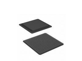
Xilinx Field Programmable Gate Array, Part #: XC5VLX30-2FF676I| FPGA | DEX
Xilinx Field Programmable Gate Array, Part #: XC5VLX30-2FF676I| FPGA | DEX
Couldn't load pickup availability
The Xilinx FPGA XC5VLX30-2FF676I Virtex-5 family contains five distinct platforms (sub-families), the most choice offered by any FPGA family. Each platform contains a different ratio of features to address the needs of a wide variety of advanced logic designs. In addition to the most advanced, high-performance logic fabric, Virtex-5 FPGAs contain many hard-IP system level blocks, including powerful 36-Kbit block RAM/FIFOs, second generation 25 x 18 DSP slices, SelectIO™ technology with built-in digitally-controlled impedance, ChipSync™ source-synchronous interface blocks, system monitor functionality, enhanced clock management tiles with integrated DCM (Digital Clock Managers) and phase-locked-loop (PLL) clock generators, and advanced configuration options
Five platforms LX, LXT, SXT, TXT, and FXT
− Virtex-5 LX: High-performance general logic applications
− Virtex-5 LXT: High-performance logic with advanced serial
connectivity
− Virtex-5 SXT: High-performance signal processing
applications with advanced serial connectivity
− Virtex-5 TXT: High-performance systems with double
density advanced serial connectivity
− Virtex-5 FXT: High-performance embedded systems with
advanced serial connectivity
• Cross-platform compatibility
− LXT, SXT, and FXT devices are footprint compatible in the
same package using adjustable voltage regulators
• Most advanced, high-performance, optimal-utilization,
FPGA fabric
− Real 6-input look-up table (LUT) technology
− Dual 5-LUT option
− Improved reduced-hop routing
− 64-bit distributed RAM option
− SRL32/Dual SRL16 option
• Powerful clock management tile (CMT) clocking
− Digital Clock Manager (DCM) blocks for zero delay
buffering, frequency synthesis, and clock phase shifting
− PLL blocks for input jitter filtering, zero delay buffering,
frequency synthesis, and phase-matched clock division
• 36-Kbit block RAM/FIFOs
− True dual-port RAM blocks
− Enhanced optional programmable FIFO logic
− Programmable
- True dual-port widths up to x36
- Simple dual-port widths up to x72
− Built-in optional error-correction circuitry
− Optionally program each block as two independent 18-Kbit
blocks
• High-performance parallel SelectIO technology
− 1.2 to 3.3V I/O Operation
− Source-synchronous interfacing using ChipSync™
technology
− Digitally-controlled impedance (DCI) active termination
− Flexible fine-grained I/O banking
− High-speed memory interface support
• Advanced DSP48E slices
− 25 x 18, two’s complement, multiplication
− Optional adder, subtracter, and accumulator
− Optional pipelining
− Optional bitwise logical functionality
− Dedicated cascade connections
• Flexible configuration options
− SPI and Parallel FLASH interface
− Multi-bitstream support with dedicated fallback
reconfiguration logic
− Auto bus width detection capability
• System Monitoring capability on all devices
− On-chip/Off-chip thermal monitoring
− On-chip/Off-chip power supply monitoring
− JTAG access to all monitored quantities
• Integrated Endpoint blocks for PCI Express Designs
− LXT, SXT, TXT, and FXT Platforms
− Compliant with the PCI Express Base Specification 1.1
− x1, x4, or x8 lane support per block
− Works in conjunction with RocketIO™ transceivers
• Tri-mode 10/100/1000 Mb/s Ethernet MACs
− LXT, SXT, TXT, and FXT Platforms
− RocketIO transceivers can be used as PHY or connect to
external PHY using many soft MII (Media Independent
Interface) options
• RocketIO GTP transceivers 100 Mb/s to 3.75 Gb/s
− LXT and SXT Platforms
• RocketIO GTX transceivers 150 Mb/s to 6.5 Gb/s
− TXT and FXT Platforms
• PowerPC 440 Microprocessors
− FXT Platform only
− RISC architecture
− 7-stage pipeline
− 32-Kbyte instruction and data caches included
− Optimized processor interface structure (crossbar)
• 65-nm copper CMOS process technology
• 1.0V core voltage
XLX:XC5VLX30-2FF676I
XC5VLX30-2FF676I


